Growth of Tin Halide Perovskite Film on Two-Dimensional Hexagonal Boron Nitride via Thermal Evaporation
- 저자
- Taewan Roh, Youjin Reo, Seongmin Heo, Geonwoong Park, Wonryeol Yang, Beomjoo Ham, Jehyun An, Ju-Hyun Jung, Seung-Hwa Baek, Rock-Hyun Baek, Cheol-Joo Kim*, Yong-Young Noh*
- 저널명
- ACS Energy Letters, 10, 5084-92 (2025)
- 년도
- 2025
- Link
- https://doi.org/10.1021/acsenergylett.5c02309 213회 연결
[Abstract]
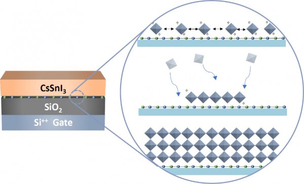
Tin halide perovskites have served as channel materials for p-type transistors owing to their low hole effective mass and suitable hole density. However, they suffer from uncontrolled film crystallization, leading to excessive tin vacancies and self-p-doping. In this study, we report a facile way to grow three-dimensional (3D) tin halide perovskite films by thermal evaporation on a dangling-bond-free hexagonal boron nitride (hBN) surface. The hBN, transferred onto SiO2 as a gate dielectric/channel interlayer, offers a hydrophobic surface that promotes the crystallization of CsSnI3 films by reducing the nucleation site density, increasing the nuclei size, and promoting the formation of uniformly oriented enlarged grains. CsSnI3 films grown on hBN exhibit reduced pinholes and grain boundaries, reducing the concentration of tin vacancies. Thin-film transistors using these films demonstrate accelerated charge transport with large current modulation without any additives. The proposed strategy can facilitate the engineering of defect-free perovskite channel layers for integrated perovskite electronics.
